Hardware Overview
The design is intentional - Just the FPGA, Flash memory, a USB-C port for power and loading circuits, and Basics Input/Output.
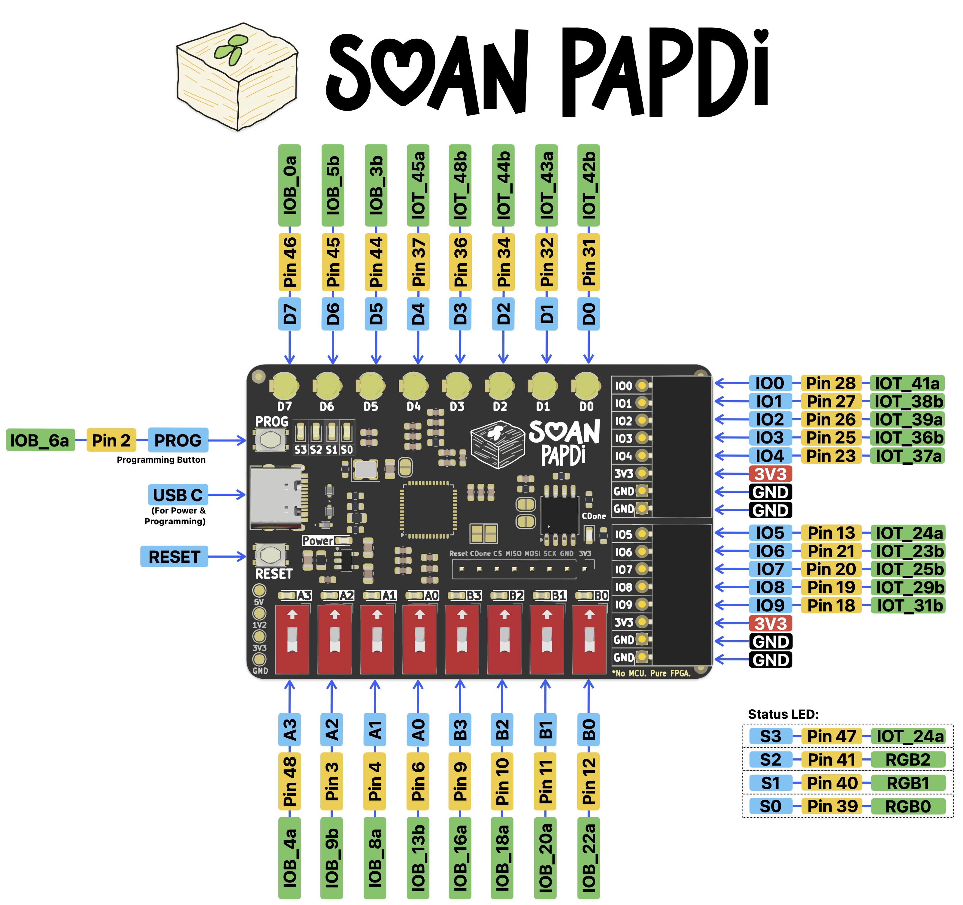
Pin Diagram
A quick roadmap of the board:
Tech Specs at a Glance
Here’s the technical rundown of what’s under the hood.
LUTs (Look-Up Tables) are the basic building blocks used to create digital circuits on an FPGA. With 5,280 of them, you have plenty of room for creative projects!
Board Tour
Let’s take a closer look at the different parts of the board:
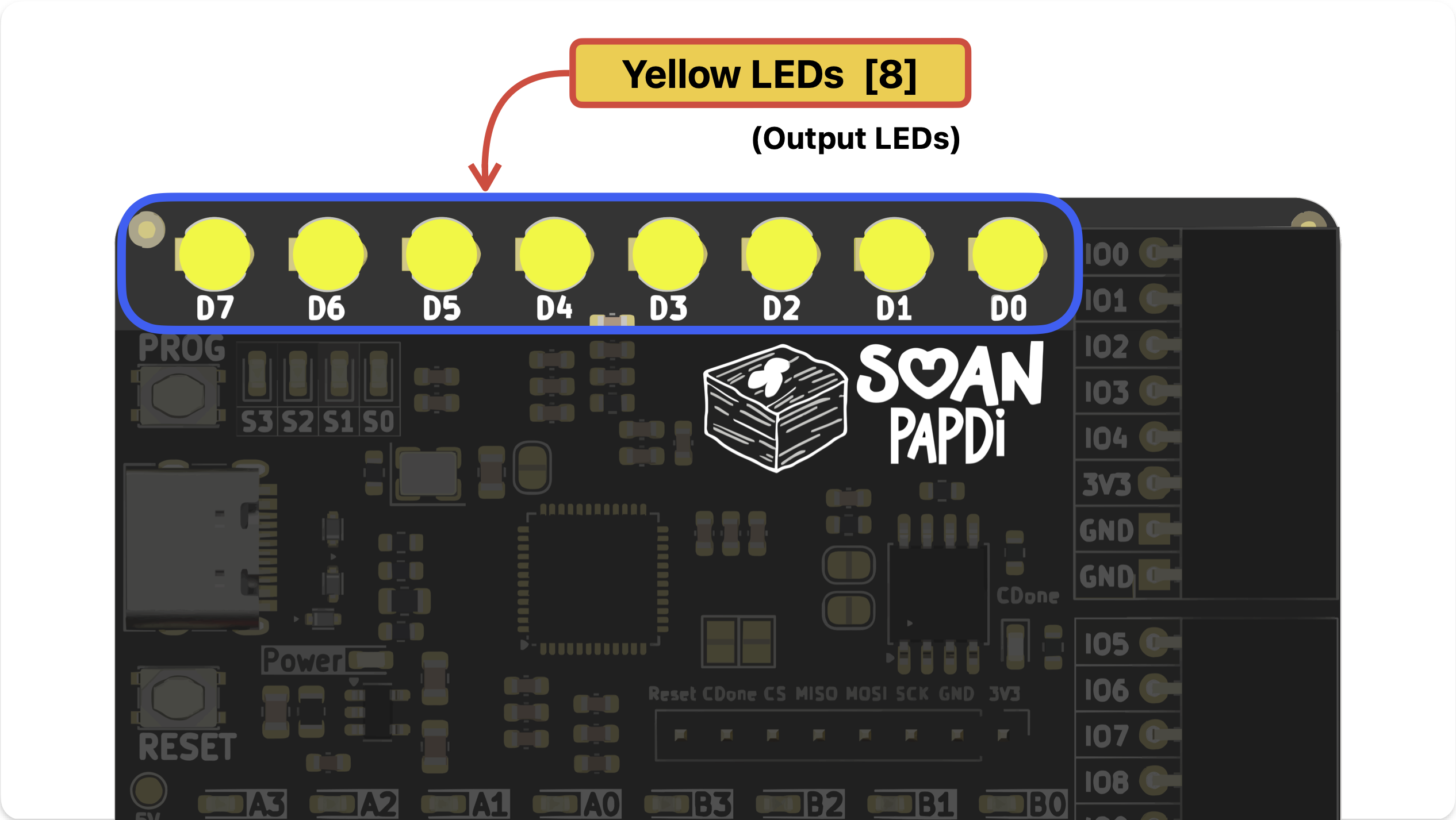
Output LEDs (D7–D0)
Along the top edge, you’ll find 8 Output LEDs (labeled D7 through D0). You can program these to light up and show the results of your circuits.
Note: These are active high, which means sending a “1” in your code turns them on.
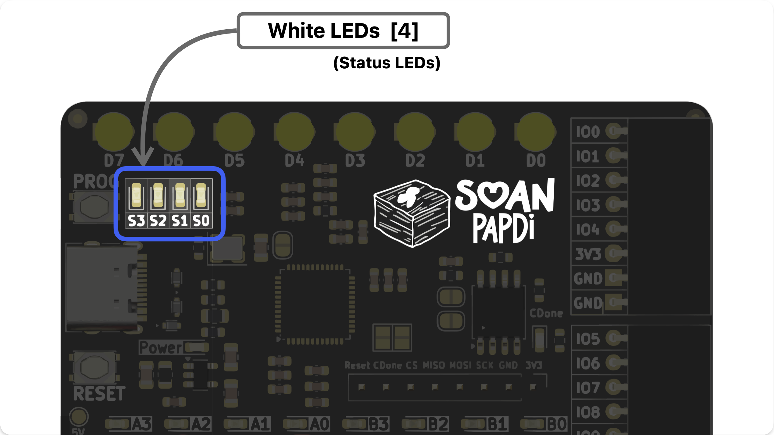
Status LEDs (S3–S0)
Right next to the main outputs are 4 White Status LEDs. These are perfect for indicating the health or current state of your design.
Note: Unlike the main LEDs, these are active low, meaning sending a “0” turns them on.
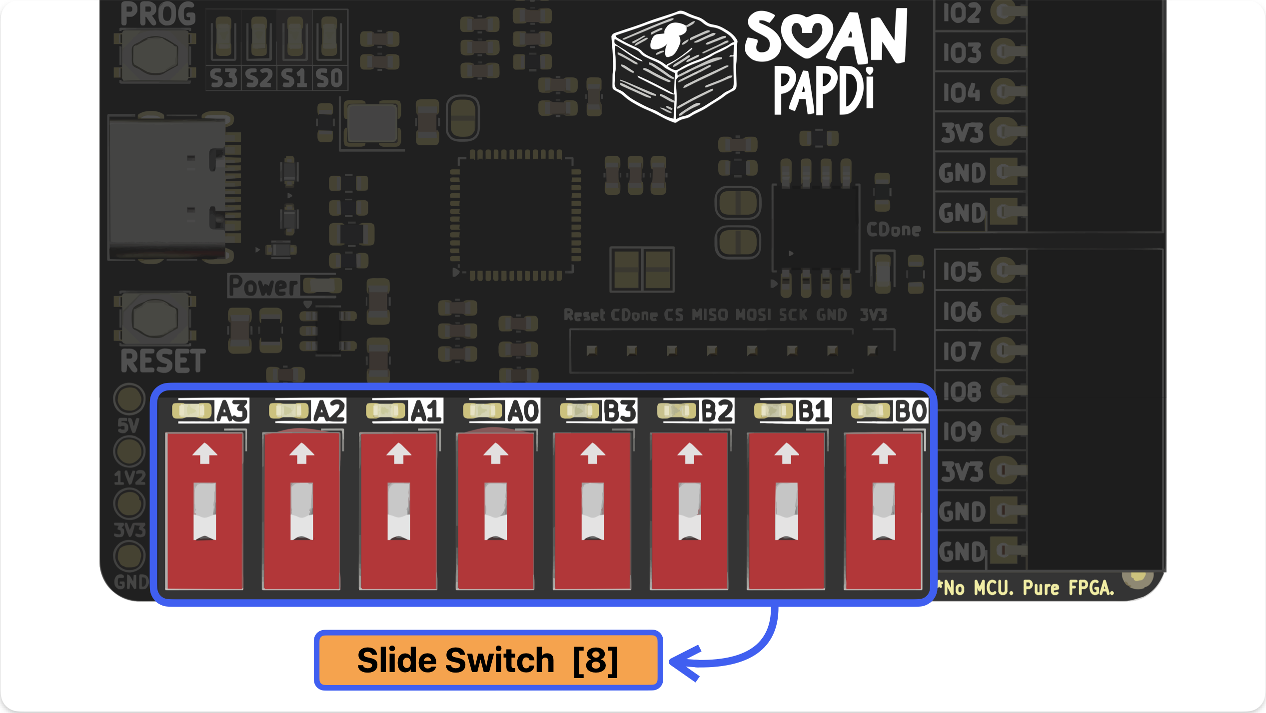
Input Switches (A3–A0 & B3–B0)
At the bottom, we’ve included 8 Slide Switches split into two groups (Set A and Set B). These are your primary way to manually send inputs (1s and 0s) directly into your FPGA designs.
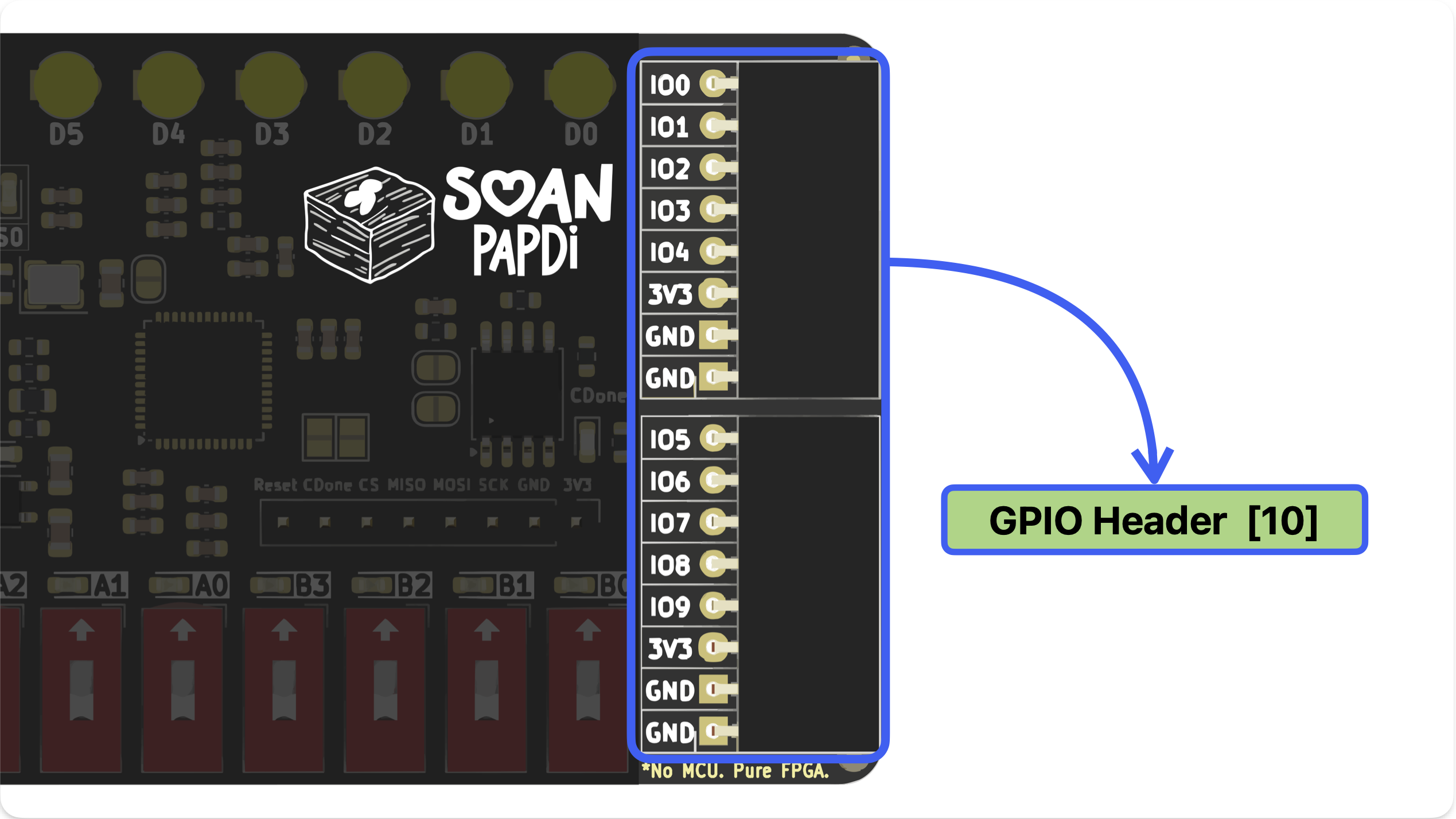
GPIO Pins (IO0–IO9)
Want to connect external sensors, motors, or displays? The right side of the board features 10 General Purpose Input/Output (GPIO) pins, allowing you to expand your projects far beyond the onboard hardware.
Datasheet
For those who want to dive deep into the lowest-level details of the FPGA chip itself: